Pioneering a New Approach to Additive Manufacturing

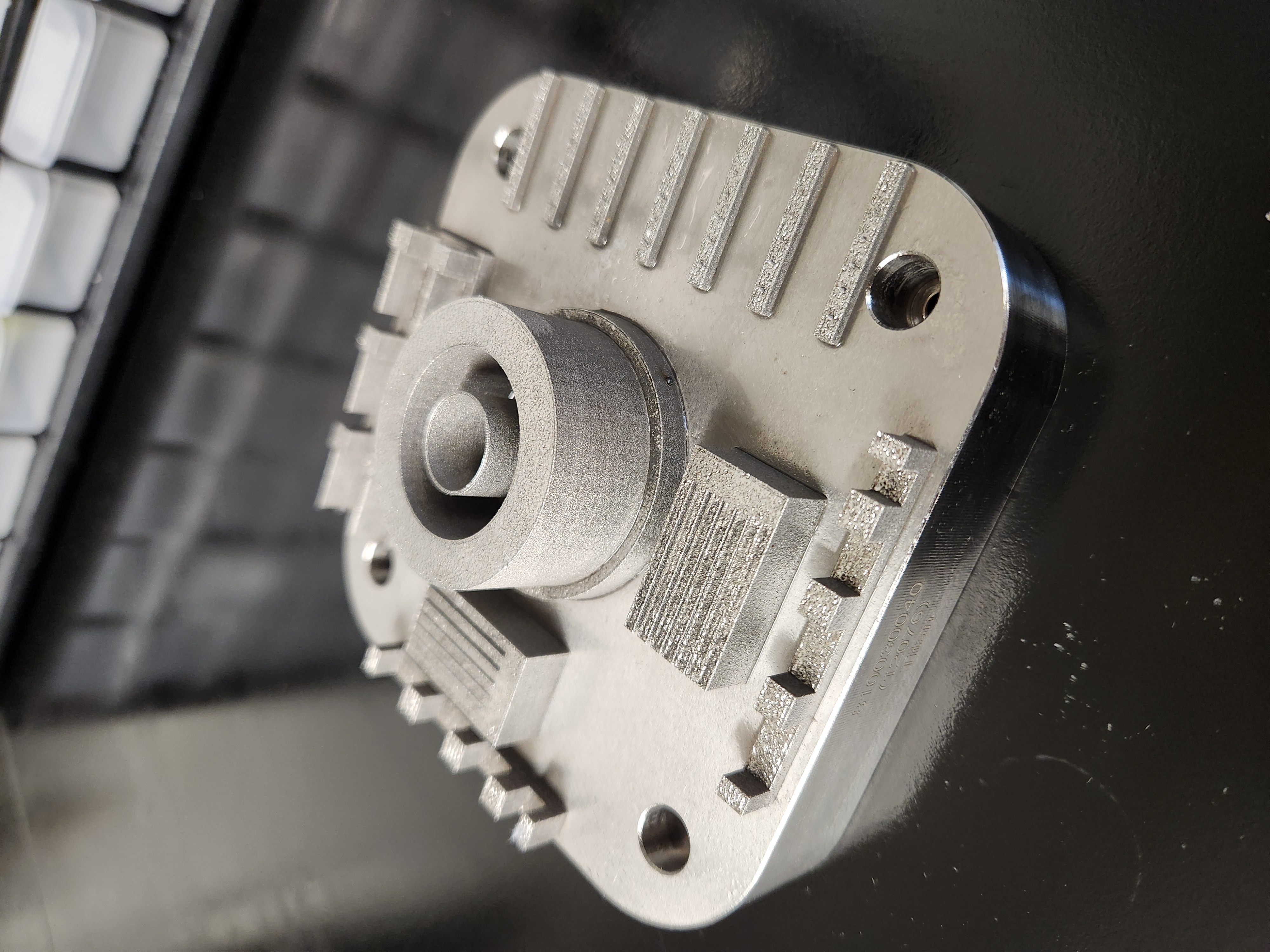
An artifact build produced by the Pantex Plant’s Technology Development and Hardin-Simmons University Team using Additive Manufacturing and promising Machine Learning.
Referred to by names such as 3D printing, freeform manufacturing, and additive manufacturing (AM), this innovative process is reshaping global manufacturing. Employing a technique that involves layering various materials facilitates the creation of intricate parts and components with high precision.
AM originated in the 1980s with American inventor Chuck Hull. The first commercial rapid 3D prototyping technology, the process was called stereolithography, which uses UV lasers to create 3D objects layer by layer. Initially used for prototyping, AM has since evolved into various techniques under 3D printing. Johannes F. Gottwald, in 1971, received the first 3D patent for the Liquid Metal Recorder, (U.S. Patent 3596285A) a continuous inkjet metal material device to form a removable metal fabrication on a reusable surface for printing by remelting material. In 2019, the accuracy, repeatability, and material range of AM evolved to the point that AM was considered viable as an industrial production technology reducing energy use by 25 percent and cutting waste and materials costs up to 90 percent. As such, AM has found applications in biomedical, aerospace, automotive, and power sector industries.
The Nuclear Security Enterprise (NSE) demands and expects as much precision, efficiency, strength, and speed as possible. So, there is always room for improvement.
The AM process has presented some inherent challenges — voids, or defects, developed in the laser melting build of each layer. These voids go undetected until the part or component is tested when failure of the part or component is evidenced. With this failure, the part or component must be discarded and the process of making a new part or component must begin again. This process results in waste of materials, energy to run the equipment, and production time.
The Pantex Plant’s Technology Development, a team of committed engineers, scientists, and technicians who support production, security, and technical infrastructure improvements, was ready for the challenge. A significant portion of Technology Development’s efforts is dedicated to applied research, aimed at translating theoretical opportunities for practical applications.
“We aim to be technology enablers for production and plant support,” explained Technology Development Director Ben Stallwitz. “Our projects work to establish capabilities which support and enhance range of Pantex mission objectives where our broader plant population excels.”
What if? This was the question that Technology Development asked to improve the AM process.
What if it were possible to identify imperfections during the manufacturing process? Imprecise component builds could be abandoned early in the time-consuming layering process. Further, what if the machine’s software could learn ways to improve itself so future component builds became more precise, more efficient, stronger, and faster with each succeeding generation?
“That’s the holy grail,” explained Senior Technical Advisor Stephen Jones, “to save time, material, and money.”
Working in partnership with Hardin-Simmons University (HSU) in Abilene, TX, the Pantex team developed an algorithm using machine learning (ML) software to do just that. This ML algorithm was developed to detect defects using the data from the photodiodes and computed tomography (CT) scans. The algorithm can be broken into three steps — 1) part separation, 2) part segmentation, and 3) defect detection.
A dataset was created to train the model using the CT scans as a way to label the defects in the part segments. The training set had an overall accuracy greater than 95 percent with defect detection accuracy of approximately 30 percent.
For the validation, the overall accuracy decreased to 80 percent and the defect detection accuracy fell to 20 percent. The validation parts were from a separate build showing that the model has the ability to predict defects across multiple builds. Currently the model used was a convolutional neural network (CNN) with plans to try other models, such as recursive neural networks (RNN). The benefit to using a RNN over CNN is that a RNN takes in variable input sizes. A variable input size is appealing because the number of datapoints in a part segment varies based on location and part geometry.
The Pantex team utilizes a SLM125 Lpbf system, Sigma Labs Printrite 3D system, and the software’s open-library format to tailor a final software product perfectly suited to Pantex and, eventually, possibly other NSE sites.
Sigma Labs has developed a methodology that mines and identifies thermal signatures of the melt pool disturbances and respective discontinuities using emission spectroscopy. Thermal signatures are defined as in-process quality metrics™ (IPQMs ®) that indicate process anomalies and inconsistencies. The system is equipped with a dual photodiode system, each with a band-pass filter with transmission chromatics of two different wavelengths. These wavelengths were chosen due to the distance from prominent emission lines of metals commonly used in AM processes.
“We have been able to take their [software] libraries and custom-build to our needs,” Jones stated.
The algorithm applies real-time responses to parts as they are built, layer upon layer. Melt pool monitoring with thermal imaging determines if the melt pool is too hot or too cold but cannot detect or predict defects or voids in the part. With ML, each layer is monitored using thermal images overlayed with CT scans to identify voids in the melt pool. Using data from each build, the computer model assigns a numerical value between one and four to any suspected voids it finds in the manufactured component. The ML technology takes in all of the data produced from the algorithm and the thermal and CT scans to learn how to identify voids or defects before applying the next layer of metal.
“It’s a recursive neural network,” Jones reveals, “an algorithm that looks at data sequentially. It takes thermal data and matches it up to the build, scan speed and images.”
“We’re teaching the system to find those ‘ones,’” he explained, “and map that defect and say, ‘is that in a critical or noncritical area?’”
As a member of the Additive Coordination Team, Pantex is collaborating with Sandia National Laboratory, Livermore National Laboratory, Kansas City National Security Campus, and Y-12 National Security Complex, sharing all aspects of AM capabilities. Oak Ridge National Laboratory has developed a software program called “Peregrine” which Pantex and HSU are using to further diagnostic capabilities for defect detection of AM metal components.
Pantex provides the HSU student researchers specifications, or parameters, for a part, tool, or component. From there, the additive-build process takes place at the university and the item is shipped out for intense scans and testing. Developing the relationship with HSU provides an opportunity for Pantex to utilize the professors, students, and lab space. This relationship develops student learning and will, potentially, offer students an opportunity to further their professional development at Pantex, if they desire.
“All the metallurgical aspects are done here at Pantex. We take the scanned images and feed that data back to the algorithm,” Jones said, “And having access to HSU’s engineering students and faculty resources allows us to send them changes and they can change the parameters in a day.”
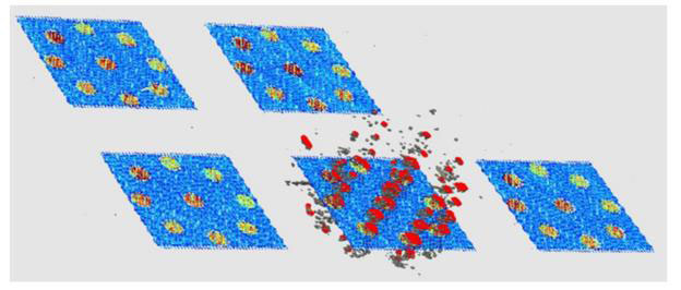
The initial thermal images and CT scans are first overlayed on top of the IPQM data to observe correlations between the in-situ data captured and the true porosity located within the part. The overlayed data can be seen in a 3D representation that displays both the IPQM data at the selected layer, and porosity.

A 3D representation that displays both the porosity and the IPQM data at a designated layer of a part.
Based on this initial ML algorithm, the model is able to predict areas of porosity from potential keyholing. A keyhole is created when the laser beam is melting and vaporizing material (metal) and the bottom of the melt pool is a vapor-filled cavity. As the laser interacts with the vapor and plasma within the keyhole, deeper penetration is allowed with the layer.
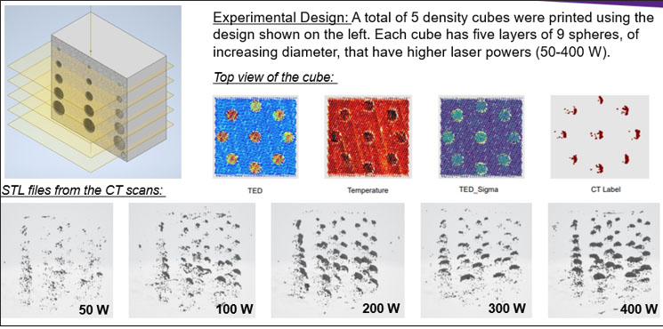
As part of the ML, the team-built spheres of various sizes and different laser power settings, as shown in the figure below, into density cubes to verify the Sigma Labs thermal images could capture those spheres. Then, CT scanned the cubes to overlay the thermal images for accuracy of predicted patterns. Although this was initially thought to provide a good learning model, a ML programmer pointed out if the model is taught to detect a forced defect, it will only learn that defect. The team is now taking as-built components and developing algorithms to look for defects based upon thermal images. This process of ML is a progressive venture. Each build and test of the algorithm provides more data to feed into the model.

Thermal images and CT scan locations of built-in porosity at different laser power settings
Currently, the ML/AM system is operating at between 50 to 60 percent accuracy rate. Not bad, but not quite where the technology needs to be for full operation. So, just how good is this algorithm likely to be?
“The endgame is to get at least 85 percent accuracy in our defect rate,” Jones said. “We keep training the model. It begins to learn. We think with that we could put a system into production that would be able to predict defects accurately.”
“This ML/AM research has the potential to change production of critical components by reducing waste, increasing efficiency of production, and reducing overall cost of production,” said Caleb Heltenberg, Pantex Plant Directed Research and Development and Partnerships and Tech Transfer Programs manager, “And, not just for Pantex and other NSE sites and labs, but it has potential applications in private industry.”
